


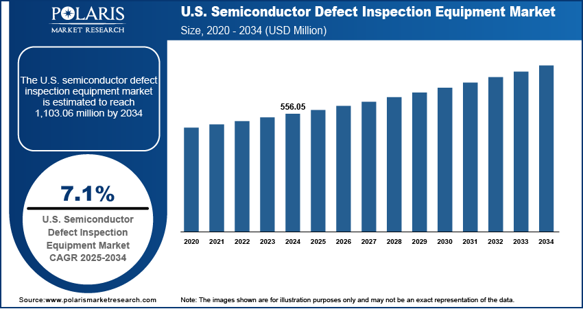
The U.S. semiconductor defect inspection equipment market, valued at USD 556.05 million in 2024, is anticipated to grow at a CAGR of 7.1% from 2025 to 2034, with segment-wise performance revealing distinct growth trajectories across product types, applications, and end-user industries. The market is segmented primarily by technology into optical inspection, electron beam (e-beam) inspection, and X-ray-based systems, each serving specific stages of the semiconductor manufacturing process. Optical inspection systems dominate in terms of revenue share, owing to their high throughput and suitability for front-end-of-line (FEOL) and back-end-of-line (BEOL) applications, particularly in logic and memory wafer fabrication.
These systems are increasingly incorporating deep ultraviolet (DUV) illumination and advanced algorithms to detect pattern anomalies at sub-10nm nodes, supporting application-specific growth in high-performance computing and AI accelerators. E-beam inspection, while slower, offers superior resolution and is critical for mask writing verification, defect review, and process development, making it indispensable for advanced logic nodes below 5nm. Demand for e-beam tools is rising in R&D fabs and pilot lines, where precision outweighs speed, and vendors like Applied Materials and KLA are investing in multi-beam e-beam platforms to improve throughput without sacrificing sensitivity. X-ray and other metrology-integrated inspection systems are gaining traction in advanced packaging applications, including fan-out wafer-level packaging (FOWLP) and 2.5D/3D integration, where internal voids, delamination, and bump misalignment require non-destructive evaluation.
Product differentiation is increasingly achieved through software intelligence, with AI-powered defect classification, automated root cause analysis, and cloud-based fleet management platforms enhancing system utility and reducing operational burden. Value chain optimization is a growing imperative, as semiconductor manufacturers seek to minimize yield loss and reduce time-to-volume production, particularly in high-mix, low-volume environments such as automotive and industrial chips. Pricing for defect inspection equipment varies significantly by segment, with optical systems ranging from $2 million to $5 million per unit, while high-end e-beam tools can exceed $10 million, reflecting their complexity and niche application.
Read More @ https://www.polarismarketresearch.com/industry-analysis/us-semiconductor-defect-inspection-equipment-market
The logic semiconductor segment remains the largest end-user, driven by demand for CPUs, GPUs, and AI processors, while memory manufacturers—particularly in 3D NAND—are investing heavily in defect inspection to manage stacking defects and ensure cell integrity across 200+ layer structures. Opportunities exist in hybrid inspection models that combine optical and e-beam modalities for faster review, as well as in edge-based analytics that reduce data latency and improve real-time decision-making. A critical trend is the integration of inspection data into digital twin frameworks, enabling virtual process optimization and predictive maintenance. As semiconductor architectures become more heterogeneous, the need for application-specific growth in inspection capabilities will intensify, favoring vendors with modular, scalable platforms and strong software ecosystems.
The U.S. semiconductor defect inspection equipment market, valued at USD 556.05 million in 2024, is anticipated to grow at a CAGR of 7.1% from 2025 to 2034, with segment-wise performance revealing distinct growth trajectories across product types, applications, and end-user industries. The market is segmented primarily by technology into optical inspection, electron beam (e-beam) inspection, and X-ray-based systems, each serving specific stages of the semiconductor manufacturing process. Optical inspection systems dominate in terms of revenue share, owing to their high throughput and suitability for front-end-of-line (FEOL) and back-end-of-line (BEOL) applications, particularly in logic and memory wafer fabrication.
These systems are increasingly incorporating deep ultraviolet (DUV) illumination and advanced algorithms to detect pattern anomalies at sub-10nm nodes, supporting application-specific growth in high-performance computing and AI accelerators. E-beam inspection, while slower, offers superior resolution and is critical for mask writing verification, defect review, and process development, making it indispensable for advanced logic nodes below 5nm. Demand for e-beam tools is rising in R&D fabs and pilot lines, where precision outweighs speed, and vendors like Applied Materials and KLA are investing in multi-beam e-beam platforms to improve throughput without sacrificing sensitivity. X-ray and other metrology-integrated inspection systems are gaining traction in advanced packaging applications, including fan-out wafer-level packaging (FOWLP) and 2.5D/3D integration, where internal voids, delamination, and bump misalignment require non-destructive evaluation.
Product differentiation is increasingly achieved through software intelligence, with AI-powered defect classification, automated root cause analysis, and cloud-based fleet management platforms enhancing system utility and reducing operational burden. Value chain optimization is a growing imperative, as semiconductor manufacturers seek to minimize yield loss and reduce time-to-volume production, particularly in high-mix, low-volume environments such as automotive and industrial chips. Pricing for defect inspection equipment varies significantly by segment, with optical systems ranging from $2 million to $5 million per unit, while high-end e-beam tools can exceed $10 million, reflecting their complexity and niche application.
Read More @ https://www.polarismarketresearch.com/industry-analysis/us-semiconductor-defect-inspection-equipment-market
The logic semiconductor segment remains the largest end-user, driven by demand for CPUs, GPUs, and AI processors, while memory manufacturers—particularly in 3D NAND—are investing heavily in defect inspection to manage stacking defects and ensure cell integrity across 200+ layer structures. Opportunities exist in hybrid inspection models that combine optical and e-beam modalities for faster review, as well as in edge-based analytics that reduce data latency and improve real-time decision-making. A critical trend is the integration of inspection data into digital twin frameworks, enabling virtual process optimization and predictive maintenance. As semiconductor architectures become more heterogeneous, the need for application-specific growth in inspection capabilities will intensify, favoring vendors with modular, scalable platforms and strong software ecosystems.
0 Commenti
·0 condivisioni
·6 Views
·0 Anteprima